
1. Introduction to Electronic Devices
Before we dive into the nitty-gritty of your NEET syllabus, let's look at where it all started. To understand the future, you’ve got to know the past, yaar! Here are the Learning Outcomes for this entire pillar post:
- Understand the historical transition from vacuum tubes to solid-state semiconductors.
- Analyze the physical classification of metals, insulators, and semiconductors based on conductivity and energy bands.
- Explain the mechanism of charge carriers, specifically electrons and holes.
- Describe the formation and biasing (forward and reverse) of p-n junctions.
- Apply diode principles to rectification and understand special-purpose circuits.
- Differentiate between various logic gates like AND, OR, and NOT.
Back in the day (pre-1948), if you wanted to control electron flow, you had to use vacuum tubes or "valves". These were bulky glass tubes where electrons were literally "boiled" off a heated cathode and made to fly through a vacuum to reach an anode. Think of them like those massive, old-school computer monitors that took up your entire desk! They were power-hungry, needed high voltages (around $100$ V), and were about as reliable as a rainy day during a cricket match.
Then came the "solid-state" revolution in the 1930s and 40s. Scientists realised we could control charge carriers inside solid materials called semiconductors. No vacuum or heating required! These modern devices are tiny, consume very little power, and are super reliable. Today, even the old Cathode Ray Tubes (CRT) in TVs have been kicked out by sleek LCD monitors backed by solid-state electronics.
Relatable Indian Example:
Imagine trying to run a pani puri stall with a massive, noisy diesel generator that needs 15 minutes to warm up (that's your vacuum tube). Now, imagine replacing it with a tiny, silent battery pack that starts instantly (that's your semiconductor). Which one would you want for your business?
NEET Checkpoint:
Why were vacuum tubes called "valves"?
(a) They could store electrical energy
(b) They allowed current to flow in only one direction
(c) They amplified both AC and DC equally
(d) They reduced electrical resistance
✅ Answer: (b) Because they allowed electrons to flow in only one direction, from cathode to anode.
NEET Checkpoint:
What is a disadvantage of vacuum tubes compared to semiconductors?
(a) They cannot amplify signals
(b) They operate only at low voltages
(c) They are bulky and consume more power
(d) They are less sensitive to heat
✅ Answer: (c) They have a limited life, low reliability, and consume high power.
NEET Checkpoint:
Where does the supply and flow of charge carriers occur in a semiconductor device?
(a) Inside the depletion region
(b) Inside the semiconductor crystal only
(c) Through the external circuit
(d) At the junction only
✅ Answer: (c) Through the external circuit. The junction only controls the flow of carriers, but the actual supply and continuous flow happens through the external circuit.
Practice Questions:
1. Which of the following was used as a radio wave detector before semiconductor theory was fully understood?
(a) Silicon Diode
(b) Galena crystal (PbS)
(c) Pentode valve
(d) Germanium Triode
✅ Answer: (b) Galena crystal (PbS) — A naturally occurring crystal with a metal point contact was used as a detector.
2. Semiconductors operate at:
(a) High voltages (~1000 V)
(b) Only at 0 K
(c) Low voltages
(d) Vacuum conditions
✅ Answer: (c) Low voltages — One of their main advantages is low-voltage operation.
Key Takeaway:
The transition from bulky, high-power vacuum tubes to small, reliable solid-state semiconductors changed electronics forever. Semiconductors are efficient because the charge flow happens within the solid material, requiring no vacuum or external heating.
2. Classification based on Conductivity & Resistivity
Before we dive into the deep funda of electronics, we need to know who's who in the world of solids. We classify them based on how much they fight against current (Resistivity, $\rho$) or how much they welcome it (Conductivity, $\sigma$). Think of $\sigma$ as the "openness" of a road and $\rho$ as the heavy traffic—they are just inverses of each other: $\sigma = 1/\rho$.
Metals are the VIPs here. They have super low resistivity ($\rho \sim 10^{-2}$ to $10^{-8} \Omega \text{ m}$) and very high conductivity. It's like a smooth highway with no speed breakers! Insulators, however, are like a massive roadblock during a Mumbai monsoon. Their resistivity is sky-high ($\rho \sim 10^{11}$ to $10^{19} \Omega \text{ m}$), so current just can’t pass through.
Then come our stars: Semiconductors. They are the "middle-benchers" with intermediate conductivity ($\sigma \sim 10^5$ to $10^{-6} \text{ S m}^{-1}$). These can be Elemental (made of single atoms like $Si$ or $Ge$) or Compound (like $GaAs$ or $CdS$). It’s like the difference between a plain paratha and a stuffed veg paratha—both are great, but the compound one is a mix of different elements.
NEET Checkpoint:
What is the unit of conductivity ($\sigma$) mentioned in the sources?
(a) ohm (Ω)
(b) S m⁻¹
(c) V/m
(d) A/V
✅ Answer: (b) $\text{S m}^{-1}$ — This stands for Siemens per metre.
NEET Checkpoint:
Is Silicon ($Si$) an elemental or compound semiconductor?
(a) Compound semiconductor
(b) Elemental semiconductor
(c) Both elemental and compound
(d) None of these
✅ Answer: (b) Elemental semiconductor — It's a pure element from the periodic table.
NEET Checkpoint:
Which material class has a resistivity range of $10^{11}$ to $10^{19} \Omega \text{ m}$?
(a) Conductors
(b) Semiconductors
(c) Insulators
(d) Superconductors
✅ Answer: (c) Insulators — High resistivity means they are very stubborn about letting current pass.
Practice Question:
A material has a conductivity of $10^4 \text{ S m}^{-1}$. Based on the indicative ranges, it is:
(a) An Insulator
(b) A Metal
(c) A Semiconductor
(d) A Polymer
✅ Answer: (c) A Semiconductor — Its value falls right into the $10^5$ to $10^{-6} \text{ S m}^{-1}$ intermediate range.
Key Takeaway
Formula Summary
- Relation: $\sigma = \frac{1}{\rho}$
- Metals: $\rho \approx 10^{-2} - 10^{-8} \Omega \text{ m}$
- Semiconductors: $\rho \approx 10^{-5} - 10^{6} \Omega \text{ m}$
- Insulators: $\rho \approx 10^{11} - 10^{19} \Omega \text{ m}$
.
3. Energy Band Theory of Solids
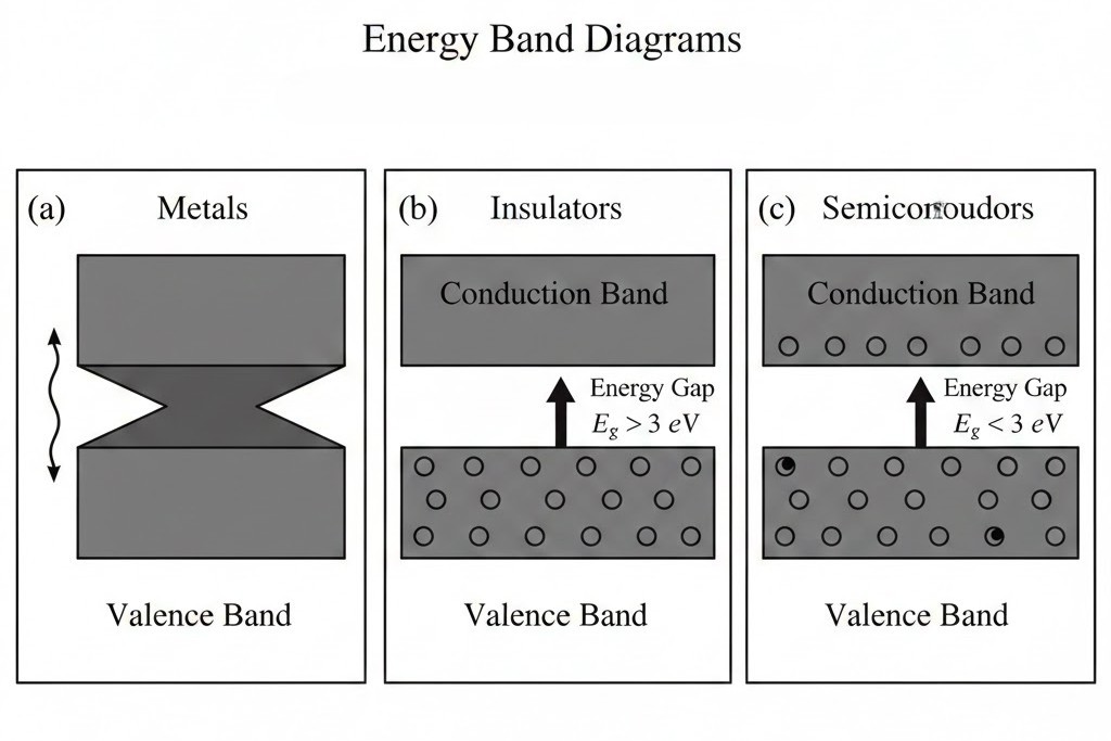
Listen up, juniors! Ever wondered why a copper wire conducts electricity like a pro while a piece of wood just sits there? It’s all about the energy band funda. Inside a solid, atoms are packed so closely that their outer electron orbits overlap, changing the nature of electron motion compared to isolated atoms. Because no two electrons see the exact same environment of surrounding charges, each electron ends up with a unique energy level. These closely spaced levels form what we call energy bands. The band containing valence electrons is the Valence Band (VB), while the one above it is the Conduction Band (CB). Normally, the CB is empty, and electrons only hang out in the VB unless they get some extra energy.
The "forbidden" zone between the top of the VB and the bottom of the CB is the Energy Band Gap ($E_g$). Think of it like a stadium: the VB is the crowded general stands, and the CB is the open pitch where you can run freely.
- Metals: The gates are wide open! Either the CB is partially filled, or the VB and CB actually overlap. This makes plenty of electrons available to move around easily.
- Insulators: These have a massive "wall" between the stands and the pitch, with a large gap of $E_g > 3\text{ eV}$. Even thermal energy isn't enough to kick electrons across this gap.
- Semiconductors: Here, the gap is small and finite, usually $E_g < 3\text{ eV}$. At room temperature, some lucky electrons gain enough thermal energy to leap into the CB, allowing a bit of conduction.
Figure below:
A clear three-part diagram showing (a) Metals with overlapping valence and conduction bands, (b) Insulators with a large energy gap $E_g > 3\text{ eV}$, and (c) Semiconductors with a small energy gap $E_g < 3\text{ eV}$.
NEET Checkpoint:
In which material is the conduction band normally empty at $0\text{ K}$?
(a) Conductors
(b) Both Insulators and semiconductors
(c) Only semiconductors
(d) Only insulators
✅ Answer: (b) Both insulators and semiconductors — Without thermal energy, no electrons can jump the gap.
NEET Checkpoint:
What happens to the gap in metals?
(a) It becomes very large
(b) It becomes moderate
(c) It is nearly zero or overlapping
(d) It fluctuates with temperature
✅ Answer: (c) It is zero or overlapping — This allows for high conductivity.
NEET Checkpoint:
If a solid has $E_g = 1.1\text{ eV}$, what is it?
(a) Conductor
(b) Semiconductor
(c) Insulator
(d) Superconductor
✅ Answer: (b) A semiconductor — This specifically describes Silicon!
Practice Questions:
- Carbon (Diamond), Silicon, and Germanium all have 4 valence electrons. Why is Diamond an insulator?
(a) It has a small $E_g$
(b) It has a very large $E_g \approx 5.4\text{ eV}$
(c) Its bands overlap
(d) It has no valence band
✅ Answer: (b) — A gap of $5.4\text{ eV}$ is way higher than $3\text{ eV}$, making it an insulator.
2. At room temperature, the resistance of a semiconductor is:
(a) Higher than an insulator
(b) Lower than a metal
(c) Intermediate between metals and insulators
(d) Zero
✅ Answer: (c) — Because of the small $E_g$, it conducts better than insulators but worse than metals.
Key Takeaway:
- Metals: Overlapping bands or partially filled CB ($E_g \approx 0$).
- Insulators: Large gap ($E_g > 3\text{ eV}$).
- Semiconductors: Small finite gap ($E_g < 3\text{ eV}$).
4. Intrinsic Semiconductors
Listen yaar, intrinsic semiconductors are the "Sanskari" kids of the electronics world—totally pure and free from any impurities like Silicon (Si) or Germanium (Ge). These guys have a diamond-like structure where every atom is bonded to four neighbours via covalent bonds.
At a chilling $T = 0\text{ K}$, they behave just like insulators because all electrons are locked up in their bonds. But as the temperature rises, thermal energy acts like a spicy pani puri—it gets things moving! This thermal excitation breaks some covalent bonds, setting electrons free to wander the lattice.
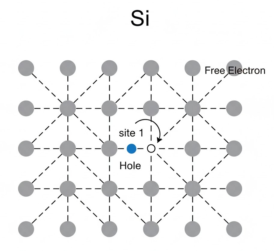
When an electron leaves its "seat" in the bond, it creates a vacancy called a hole. Think of a crowded bus: if someone stands up, the empty seat (hole) can "move" if the person next to them slides over to take it! This hole behaves like an effective positive charge ($+q$).
In these pure crystals, every free electron leaves exactly one hole behind, so the carrier concentrations are always equal:
where $n_i$ is the intrinsic carrier concentration.
NEET Checkpoint:
At absolute zero, an intrinsic semiconductor acts as:
(a) A perfect conductor
(b) An insulator
(c) A semiconductor
✅ Answer: (b) — $0\text{ K}$, no thermal energy is available to break bonds, so no free charges exist!
The cool part? Both electrons and holes contribute to the flow! While free electrons zip around, holes "move" as bound electrons hop into vacancies. The total current $I$ is the sum of the electron current ($I_e$) and the hole current ($I_h$):
NEET Checkpoint:
What is a hole?
(a) A proton
(b) An empty space in a conductor
(c) An effective positive charge carrier
✅ Answer: (c) — It is a vacancy in a covalent bond that behaves like a positive charge.
Figure below:
A 2D schematic diagram of a Silicon crystal lattice showing covalent bonds. One bond is broken, showing a 'free electron' moving away and a 'hole' (empty circle) left at the bonding site, labeled 'site 1'.
NEET Checkpoint:
If an intrinsic semiconductor has $10^{16}$ free electrons per $m^3$, how many holes does it have?
(a) 0
(b) Cannot be determined
(c) 2 × 10¹⁶ per m³
(d) 10¹⁶ per m³
✅ Answer: (d) $10^{16}$ per $m^3$ — In intrinsic materials, $n_e$ must equal $n_h$.
Practice Question:
In an intrinsic semiconductor, why does the conductivity increase with temperature?
(a) Holes and electrons recombine faster.
(b) More covalent bonds break due to thermal energy.
(c) The energy gap $E_g$ becomes zero.
(d) The lattice structure changes to a metal.
✅ Answer: (b) — Higher temperature provides more thermal energy to excite electrons from the valence band to the conduction band.
Now that you've mastered the pure stuff, let’s see what happens when we intentionally add some "spice" to the mix!
Key Takeaway
Formula Summary
- Carrier Equality: $n_e = n_h = n_i$
- Total Current: $I = I_e + I_h$
- Charge of a Hole: $+q$ (effective)
5. Extrinsic Semiconductors: n-type Materials
Listen, junior, intrinsic semiconductors are okay for textbooks, but in the real world, their room-temperature conductivity is just too low to build anything cool. To fix this, we use a process called doping, which is basically adding a "tadka" of specific impurity atoms (dopants) to the pure crystal to boost its conductivity manifold. For n-type materials, we use pentavalent dopants—elements from Group V like Arsenic ($As$), Antimony ($Sb$), or Phosphorus ($P$).
NEET Checkpoint:
Why do we dope semiconductors?
(a) To increase their size
(b) To make them transparent
(c) To increase their conductivity
(d) To reduce their melting point
✅ Answer: (a) To increase conductivity—Pure Si/Ge at room temp just doesn't have enough free carriers to be useful.
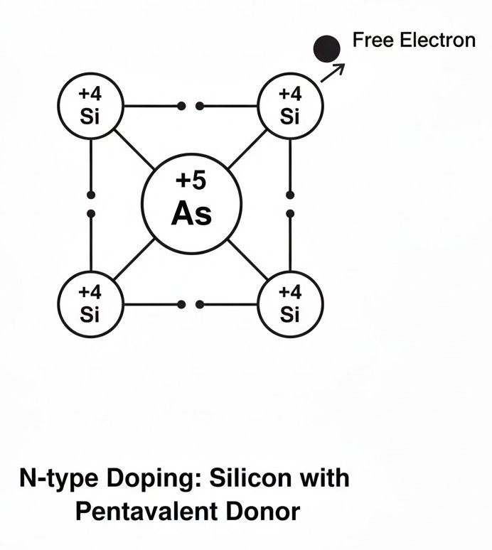
Here is the funda: when a pentavalent atom takes the place of a $Si$ atom in the lattice, four of its electrons form covalent bonds with neighbors, but the fifth electron is left out in the cold. This extra electron is very weakly bound; it only needs about $0.01 \text{ eV}$ in $Ge$ or $0.05 \text{ eV}$ in $Si$ to break free and start conducting. It’s like a local cricket team bringing in a "pro" guest player who doesn't need to follow the usual practice rules—he's ready to hit boundaries (conduct) immediately!
NEET Checkpoint:
Which of these is a donor impurity?
(a) $B$
(b) $Al$
(c) $In$
(d) $P$
✅ Answer: (d) $P$ — Phosphorus is pentavalent and "donates" an electron.
In these materials, electrons become the majority carriers ($n_e$), while holes are the minority carriers ($n_h$). Because the dopant "donates" an electron, it's called a donor impurity. Even though we have so many extra electrons, remember that the crystal stays electrically neutral because the charge of the extra electrons is balanced by the positive charge of the ionised donor cores.
Figure below:
A clear diagram showing a central +5 pentavalent donor atom (like As) surrounded by four +4 Silicon atoms, with four covalent bonds formed and one 'unbonded' free electron moving away from the donor site.
NEET Checkpoint:
What is the carrier condition for n-type?
(a) $ n_e ≫ n_h $
(b) $n_e ≪ n_h$
(c) $n_e ≈ n_h$
(d) Only holes are present
✅ Answer: (a) $n_e \gg n_h$ — The number of conduction electrons is much larger than the number of holes.
Practice Questions:
1. The ionisation energy required to set the fifth electron free in a doped silicon crystal is approximately:
(a) $1.1 \text{ eV}$
(b) $0.72 \text{ eV}$
(c) $0.05 \text{ eV}$
(d) $0.01 \text{ eV}$
✅ Answer: (c) — As per the sources, $Si$ needs ~ $0.05 \text{ eV}$ while $Ge$ needs ~ $0.01 \text{ eV}$.
2. In an n-type semiconductor, the minority carriers are:
(a) Electrons
(b) Holes
(c) Pentavalent atoms
(d) Photons
✅ Answer: (b) — Electrons are donated in bulk, making holes the rare minority.
Key Takeaway & Formula Summary
- Doping: Adding impurities (ppm) to increase conductivity.
- n-type Dopants: Pentavalent ($As, Sb, P$).
- Majority Carriers: Electrons ($n_e$); Minority Carriers: Holes ($n_h$).
- Condition:
$$n_e \gg n_h$$- Mass Action Law:
$$n_e n_h = n_i^2$$
6. Extrinsic Semiconductors: p-type Materials
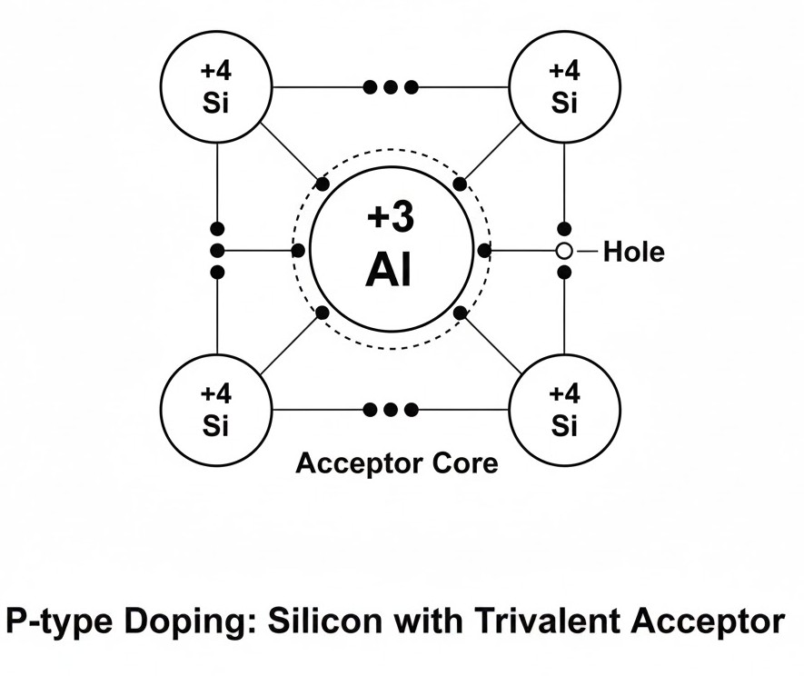
Listen, yaar, if n-type was about "extra" electrons, p-type is all about the "Positive" vibe created by vacancies! To make a p-type semiconductor, we dope pure Silicon or Germanium with trivalent impurities like Indium ($In$), Boron ($B$), or Aluminium ($Al$). These guys have only three valence electrons, which is one less than what Si or Ge needs to finish its four covalent bonds.
This creates a "vacancy" or a hole in the lattice. Since the trivalent atom is basically "accepting" an electron from a neighbor to try and complete its bond, we call it an acceptor impurity. When a neighboring electron jumps into this hole, it leaves a new hole behind—effectively making the hole move around! In these materials, holes are the majority carriers and electrons are the minority carriers.
NEET Checkpoint:
Which of the following is used as an acceptor impurity?
(a) Phosphorus
(b) Antimony
(c) Boron
(d) Arsenic
✅ Answer: (c) Boron — Remember the trio: $B, Al, In$ are our trivalent acceptor friends!.
Think of a crowded Mumbai local train where one seat is empty. As people shift to fill that "vacancy," the empty spot seems to travel through the carriage. That’s exactly how a hole conducts! Even though we have all these holes, the crystal maintains overall charge neutrality. The total positive charge of the holes is perfectly balanced by the negative charge of the ionised acceptor cores.
NEET Checkpoint:
In a p-type semiconductor, the condition for carrier concentration is:
(a) $n_e \gg n_h$
(b) $n_h \gg n_e$
(c) $n_e = n_h$
(d) $n_h = 0$
✅ Answer: (b) $n_h \gg n_e$ — Holes rule the roost here!.
Figure below:
A clear diagram showing a Silicon lattice with one Aluminium atom creating a vacancy (hole) in a covalent bond, similar to NCERT Figure 14.8, highlighting the acceptor core and the associated hole.
NEET Checkpoint:
Is a p-type semiconductor positively charged?
(a) Yes, it is positively charged
(b) No, it is negatively charged
(c) No, it is electrically neutral
(d) It depends on temperature
✅ Answer: (c) No, it is electrically neutral - It remains electrically neutral because the dopant atoms are neutral when added, and the total charge in the lattice stays balanced.
Practice Question:
A pure Si crystal is doped with Indium. What happens to the concentration of intrinsically generated electrons ($n_e$)?
(a) Increases
(b) Stays the same
(c) Decreases
(d) Becomes zero
✅ Answer: (c) Decreases — Due to the abundance of holes, the recombination process increases, which reduces the number of intrinsic electrons.
Key Takeaway: p-type Fundamentals
- Dopants: Trivalent ($B, Al, In$).
- Majority Carriers: Holes ($n_h \gg n_e$).
- Energy Level: Acceptor level $E_A$ sits slightly above the valence band $E_V$.
- Charge: Always electrically neutral.
7. p-n Junction Formation
Now we are getting to the real hero of our electronics story—the p-n junction. Think of it like a "filmy" meeting between two rival neighborhoods: the p-side (full of holes) and the n-side (packed with electrons).
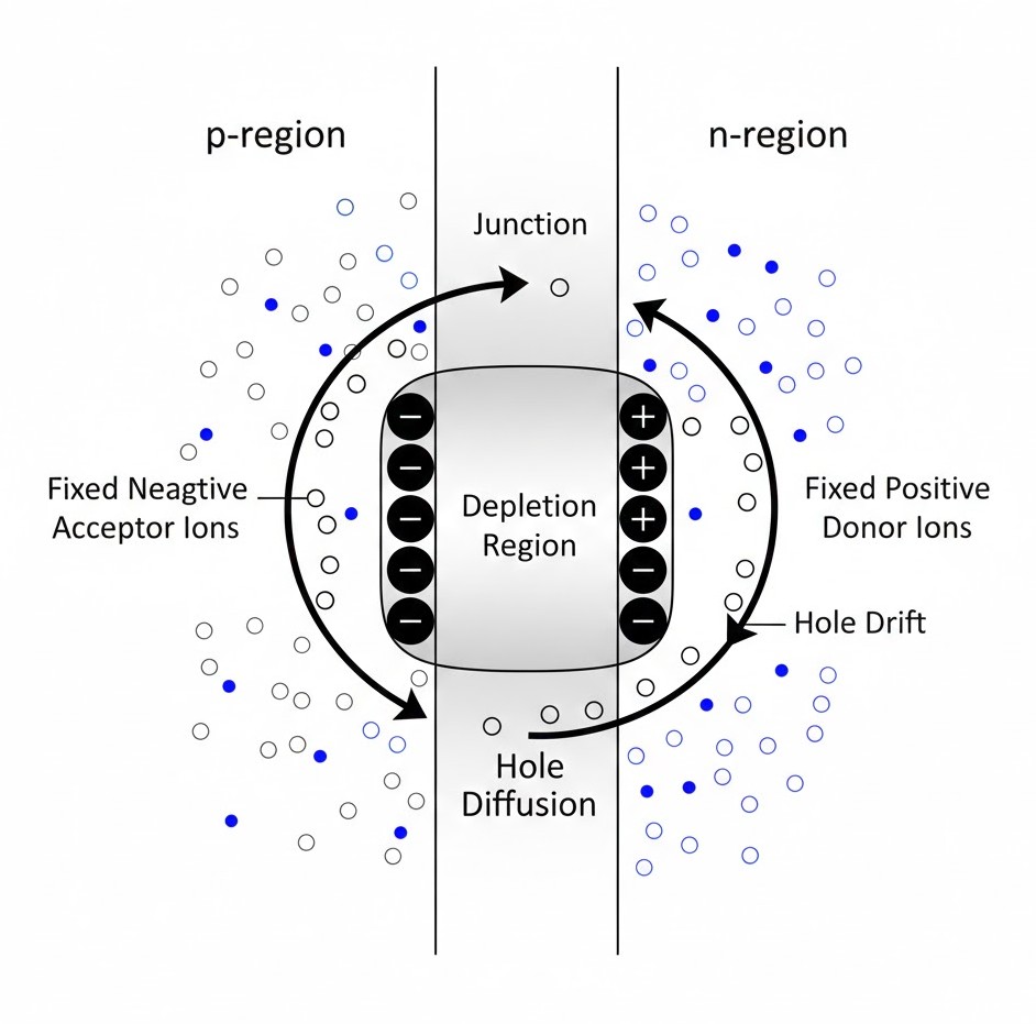
When they meet at the metallurgical junction, the electrons from the n-side see the p-side and think, "Chalo, let's go there!" This movement, triggered by the concentration gradient, is called diffusion. It’s exactly like a crowded Mumbai local train—people naturally move from the packed coach towards the empty platform! As electrons leave the n-side, they leave behind positive "angry" immobile ions. On the p-side, incoming electrons create negative immobile ions. This creates the depletion region—a "No Man’s Land" about $0.1$ $\mu m$ thick where no free carriers dare to stay.
NEET Checkpoint:
What is the approximate thickness of the depletion layer?
(a) $1$ cm
(b) $1$ mm
(c) $0.1$ $\mu m$
(d) $10$ m
✅ Answer: (c) $0.1$ $\mu m$ — It's thinner than a strand of hair, so don't let the small size fool you!.
This separation of charges creates an internal electric field directed from n to p. This field acts like a strict traffic police officer, pushing minority carriers across the junction. This field-driven movement is called drift. Initially, diffusion is high, but as the field grows, drift increases until diffusion current equals drift current. This is the equilibrium state where no net current flows, and a barrier potential ($V_0$) is established to stop any more mischief!.
NEET Checkpoint:
In an unbiased p-n junction, the net current is:
(a) Very high
(b) Zero
(c) Infinite
(d) Negative
✅ Answer: (b) Zero — Because the bouncers (drift) and the crowd (diffusion) are in a perfect tug-of-war!.
Figure below:
A clear diagram of a p-n junction showing the p-region and n-region meeting at a junction. Show the depletion region in the centre with fixed negative ions on the p-side and fixed positive ions on the n-side. Include arrows for 'Hole Diffusion' from p to n and 'Hole Drift' from n to p.
NEET Checkpoint:
Diffusion current in a p-n junction is caused by:
(a) Heat only
(b) Electric field
(c) Concentration gradient
(d) Battery
✅ Answer: (c) Concentration gradient — Just like the smell of biryani spreading through a room!.
Practice Questions:
- During the formation of a p-n junction, the n-region becomes:
(a) Negatively charged
(b) Positively charged
(c) Neutral
(d) Insulating
✅ Answer: (b) The n-side loses electrons to the p-side, leaving behind immobile positive donor ions.
2. The direction of the drift current in a p-n junction is:
(a) From p to n
(b) From n to p
(c) Upwards
(d) Random
✅ Answer: (b) The electric field is from n to p, so it moves holes from n to p, creating a drift current in that direction.
Key Takeaway:
- Diffusion: Carriers moving $p \rightarrow n$ (holes) and $n \rightarrow p$ (electrons) due to concentration difference.
- Drift: Carriers moving due to the junction's internal electric field.
- Equilibrium: When $I_{diffusion} = I_{drift}$, resulting in a barrier potential ($V_0$).
8. Depletion Region & Barrier Potential
Listen up, junior! When you bring p-type and n-type materials together, it’s like a high-stakes cricket match where the crowd is rushing the gates. Electrons from the n-side and holes from the p-side start diffusing across the junction because of the concentration gradient.
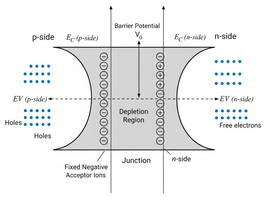
But here’s the catch: as electrons leave the n-side, they leave behind grumpy, immobile positive donor ions. On the p-side, escaping holes leave behind immobile negative acceptor ions. This "No-Man’s Land" is the Depletion Region, and it’s super thin—about $0.1\ \mu m$ (which is $10^{-7}\ m$). It’s "depleted" of free carriers, like a Pani Puri stall that’s just run out of masala!
NEET Checkpoint:
During p-n junction formation, what is the state of the n-side?
(a) Becomes negatively charged
(b) Becomes positive relative to p-side
(c) Remains neutral
(d) Becomes a conductor
✅ Answer: (b) Becomes positive relative to p-side — Because it loses its 'free' electrons, leaving behind positive ion cores!
This separation of charges creates an electric field directed from n to p, leading to a Barrier Potential ($V_0$). The n-side becomes positive relative to the p-side, acting like a bouncer at a club—no more majority carriers get through without the right energy!
Figure below:
A clear diagram of a p-n junction showing the depletion region with positive ion cores on the n-side, negative ion cores on the p-side, and the barrier potential $V_0$ shown as a step-up from p to n.
NEET Checkpoint:
What is the typical thickness of the depletion layer?
(a) $1\ mm$
(b) $10^{-6}\ m$
(c) $10^{-7}\ m$
(d) $1\ cm$
✅ Answer: (c) $10^{-7}\ m$ — The sources mention it is of the order of one-tenth of a micrometre.
At equilibrium, the diffusion current equals the drift current, and the net current is zero. Don't stress, yaar—just remember that the barrier stops the "traffic" of majority carriers!
NEET Checkpoint:
At equilibrium in an unbiased p-n junction:
(a) Diffusion current > Drift current
(b) Diffusion current = Drift current
(c) Drift current = 0
(d) No ions exist
✅ Answer: (b) Diffusion current = Drift current — This is the condition for equilibrium where no net current flows.
Practice Question:
The barrier potential ($V_0$) in a p-n junction:
(a) Assists diffusion of majority carriers
(b) Opposes diffusion of majority carriers
(c) Is zero at room temperature
(d) Decreases with reverse bias
✅ Answer: (b) Opposes diffusion of majority carriers — The polarity is such that it prevents further flow of carriers to maintain equilibrium.
Key Takeaway
- Depletion Layer: Contains immobile ionised cores and is devoid of free charges.
- Barrier Potential ($V_0$): The n-side is Positive and the p-side is Negative.
- Equilibrium: Reached when Diffusion Current = Drift Current.
9. Semiconductor Diode & Forward Bias
Listen up, junior! Now we are going to make our p-n junction actually do some work. A semiconductor diode is essentially a p-n junction with metallic contacts on both ends so we can plug it into a circuit. The symbol looks like an arrow pointing the way current likes to flow—think of it as a "one-way" street sign for electrons!
Forward bias is the "Go" signal. You connect the p-side to the positive terminal and the n-side to the negative terminal. Here’s the trick: the applied voltage $V$ acts against the built-in barrier $V_0$. This "tug-of-war" reduces the depletion layer width and lowers the barrier height to exactly $(V_0 - V)$.
NEET Checkpoint:
In forward bias, which terminal is the n-side connected to?
(a) Positive terminal
(b) Negative terminal
(c) Ground
(d) Either terminal
✅ Answer: (b) The negative terminal — Remember: N for Negative, P for Positive. Easy funda, right?
Imagine a crowded Mumbai local train platform. The barrier is like the ticket checker. If you don't have enough "energy" (a ticket), you can't pass. But with forward bias, it's like the gates opening up! At first, the current is tiny, but once you cross the threshold or cut-in voltage ($\approx 0.7\text{ V}$ for Silicon), the current increases significantly. Even a small extra "dhakka" (voltage) makes the current zoom up exponentially!
NEET Checkpoint:
What happens to the depletion layer in forward bias?
(a) It increases
(b) It decreases
(c) It remains constant
(d) It becomes infinite
✅ Answer: (b) It decreases — The applied field opposes the internal field, pushing charge carriers toward the junction.
NEET Checkpoint:
What is the typical cut-in voltage for a Silicon diode?
(a) (a) 0.1 V (b) 0.3 V (c) 0.7 V (d) 1.2 V $\approx 0.1\text{ V}$
(b) $\approx 0.3\text{ V}$
(c) $\approx 0.7\text{ V}$
(d) $\approx 1.2\text{ V}$
✅ Answer: (c) $\approx 0.7\text{ V}$ — Below this, the diode is basically "sleeping".
Practice Question :
If the applied voltage $V$ in forward bias is increased, the effective barrier height becomes:
(a) $V_0 + V$
(b) $V_0 - V$
(c) $V / V_0$
(d) No change
✅ Answer: (b) $V_0 - V$ — The external voltage "eats away" at the internal barrier.
Key Takeaway
- Forward Bias: P $\rightarrow$ (+), N $\rightarrow$ (-).
- Depletion Width: Decreases.
- Effective Barrier: $(V_0 - V)$.
- Current: Increases sharply after threshold voltage.
10. Reverse Bias & I-V Characteristics
If you connect the n-side to the positive terminal and the p-side to the negative terminal, you’ve just put the diode in Reverse Bias. It’s like trying to drive a scooty against a one-way street—the barrier height increases to $(V_0 + V)$, and that depletion region gets wider than the line at a popular Pani Puri stall!. Because the barrier is so high, the majority carriers are blocked from crossing.
NEET Checkpoint:
What happens to the depletion width in reverse bias?
(a) Decreases
(b) Increases
(c) Remains same
✅ Answer: (b) Increases — The applied voltage direction is the same as the barrier potential, pushing charge carriers further apart.
We only see a tiny Reverse Saturation Current from minority carriers, measured in microamperes ($\mu A$). This current is almost constant, like that one friend who always gives a fixed $\text{₹}10$ contribution for treats regardless of the bill. But beware: if you keep increasing the voltage, you'll hit the Breakdown Voltage ($V_{br}$). At this point, the current shoots up like a rocket, and if you don't limit it, your diode is history!.
NEET Checkpoint:
Reverse current is primarily due to:
(a) Majority carriers
(b) Minority carriers
(c) Protons
✅ Answer: (b) Minority carriers — Randomly moving minority carriers are swept across the junction by the strong electric field.
To measure how the diode resists changes, we use Dynamic Resistance ($r_d$):
figure below:
A circuit diagram showing a p-n junction in reverse bias with a battery (n-side to positive), a microammeter, and a voltmeter, along with a V-I characteristic graph showing the reverse saturation current and the sharp increase at breakdown voltage.

NEET Checkpoint:
Which unit is typically used to measure reverse current in a Si diode?
(a) $A$
(b) $mA$
(c) $\mu A$
(d) $kA$
✅ Answer: (c) $\mu A$ — Reverse current is extremely small compared to the mA seen in forward bias.
Practice Question:
At the Breakdown Voltage ($V_{br}$), a slight increase in bias voltage results in:
(a) Current reaching zero
(b) A sharp increase in current
(c) No change in current
✅ Answer: (b) A sharp increase in current — This is the critical point where the diode's reverse current is no longer independent of voltage.
Now that you've mastered the "No-Entry" zone of reverse bias, wait till you see how we use this one-way traffic trick to build a rectifier!
Key Takeaway & Formula Summary
- Connection: n-side (+), p-side (-).
- Barrier Height: Increases to $(V_0 + V)$.
- Current: Very small ($\mu A$), due to minority carriers.
- Dynamic Resistance Formula:
$$r_d = \frac{\Delta V}{\Delta I}$$
11. Application: Diode as a Rectifier
Listen up, junior! Ever wonder how your phone charger converts that messy AC from the wall into clean DC? That’s where our hero, the junction diode, enters the scene. Its "superpower" is allowing current to flow in only one direction—specifically when it is forward biased.
NEET Checkpoint:
If an AC voltage is applied to a single diode, when does it conduct?
(a) During both positive and negative half cycles
(b) Only during the negative half cycle
(c) Only during the positive half cycle
(d) It never conducts
✅ Answer: (c) Only during the half-cycle when the diode is forward biased, it's a one-way street!.
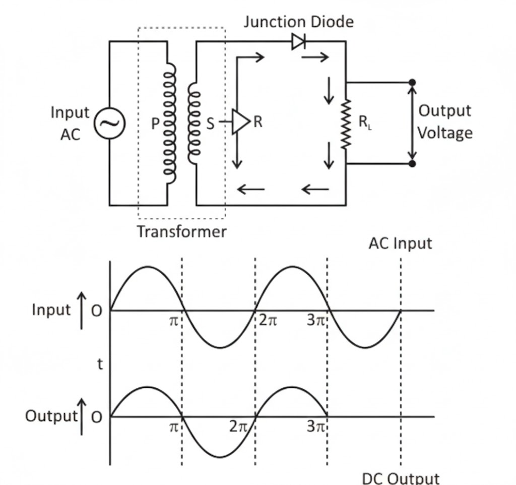
In a half-wave rectifier, we use a single diode in series with a load $R_{L}$. It’s like a pani puri vendor who only serves you when the sun is out; during the "negative" rainy half-cycle, the diode is reverse biased and shuts down, giving zero output.
Figure below:
A clear diagram showing a half-wave rectifier circuit with a transformer, a single diode, a load resistor $R_{L}$, and the corresponding input/output waveforms.
To make things efficient, we use a full-wave rectifier with two diodes and a centre-tap transformer. Here, the two diodes take turns! While $D_{1}$ handles the positive half, $D_{2}$ handles the negative half. It’s like having two rickshaws on standby so you’re never waiting in the rain.
NEET Checkpoint:
What is the output frequency of a full-wave rectifier if the input is $50~Hz$?
(a) $25~Hz$
(b) $50~Hz$
(c) $100~Hz$
(d) $200~Hz$
✅ Answer: (c) $100~Hz$ — Because we get two output pulses for every one input cycle!.
But wait, this output is "pulsating" DC. To smooth it out like a creamy lassi, we add filters—usually a large capacitor $C$ in parallel with $R_{L}$. The capacitor charges to the peak voltage and discharges slowly, maintaining a steady $V$.
NEET Checkpoint:
Which property of a capacitor helps in smoothing the output?
(a) Low resistance
(b) High inductance
(c) Ability to store charge
(d) High power rating
✅ Answer: (c) Its ability to store charge and discharge slowly based on the time constant $C R_{L}$ — Keeping the energy "funda" steady!.
Practice Questions:
1. In a full-wave rectifier, if one diode is damaged, it will behave as:
(a) An amplifier
(b) A half-wave rectifier
(c) A filter
(d) A short circuit
✅ Answer: (b) — With only one diode left, it can only rectify half the cycle!.
2. Why are capacitors used in power supplies?
(a) To increase AC
(b) To act as a resistor
(c) To filter out AC ripples
(d) To block DC
✅ Answer: (c) — They smooth the pulsating DC into a steadier value.
Key Takeaway
- Rectification: Converting AC to DC using the one-way conduction of diodes.
- Half-wave: 1 diode; lower efficiency.
- Full-wave: 2 diodes + centre-tap; higher efficiency.
- Filters: Use capacitors/inductors to remove "ripples" for a steady DC output.
12. Special Diodes: Zener Diode & Regulation
Hey there, future doc! Ever wondered how your expensive smartphone charger handles those annoying "voltage fluctuations" at home without blowing up? Let’s clear up this funda using the superhero of the semiconductor world: the Zener Diode.
The Breakdown "Magic"
While normal junction diodes are mostly used in forward bias, the Zener diode is a special-purpose diode designed to operate in the reverse breakdown region. Normally, if you push a general diode into reverse bias, it only carries a tiny micrometer $(\mu A)$ current. But once you hit a critical limit called the breakdown voltage ($V_{br}$), the current increases sharply.
Here's the trick: at this breakdown point, even a slight increase in bias voltage causes a massive change in current. This "special action" is the secret sauce for voltage regulation.
NEET Checkpoint:
In which region is a Zener diode primarily operated?
(a) Forward bias region
(b) Reverse bias (before breakdown)
(c) Reverse bias breakdown region
(d) Saturation region
✅ Answer: (c) Reverse bias breakdown region — Unlike normal diodes, Zeners are built to handle the "breakdown" without getting destroyed.
Maintaining the Balance
Imagine a local rickshaw with a speed governor. No matter how hard the driver hits the gas (input voltage fluctuations), the rickshaw won't cross $40\ km/h$ (constant output voltage). That’s exactly what a Zener does in a circuit! It maintains a constant voltage even if the input or load current fluctuates.
NEET Checkpoint:
What happens to the reverse current at $V = V_{br}$?
(a) It becomes zero
(b) It increases slowly
(c) It increases sharply
(d) It remains constant
✅ Answer: (c) It increases sharply — Even a tiny voltage change leads to a large current flow.
NEET Checkpoint:
Why are general-purpose diodes not used in the breakdown region?
(a) They stop conducting current
(b) There is a risk of overheating
(c) Their resistance becomes infinite
(d) They work only in forward bias
✅ Answer: (b) Risk of overheating — If the current isn't limited, the junction gets destroyed.
Practice Questions:
1. A special-purpose semiconductor diode used as a voltage regulator is:
(a) LED
(b) Photodiode
(c) Zener diode
(d) Solar cell
✅ Answer: (c) Zener diode — The sources explicitly list its application as a voltage regulator.
2. At the breakdown voltage ($V_{br}$), the diode current is:
(a) Zero
(b) Constant
(c) Extremely sensitive to voltage changes
(d) Negligible
✅ Answer: (c) Extremely sensitive — A slight increase in bias causes a large change in current.
Key Takeaway
Formula Summary
* Operation Point: Reverse Bias at $V = V_{br}$
* Forward Current: Measured in $mA$
* Reverse Current: Measured in $\mu A$ (until breakdown)
13. Optoelectronic Junction Devices
Arre yaar, don't think that semiconductors are just for hidden circuits! Some of them are total "show-offs" that love interacting with light. These are our optoelectronic devices. While the detailed I-V characteristics for each specific device aren't fully fleshed out in our current notes, the basic funda is simple: light is a source of energy that can kick-start the charge carriers in a junction.
Notice this: in a semiconductor, electrons are usually chilling in the valence band. But when light hits the material, these electrons can absorb that energy to jump across the energy gap ($E_g$) into the conduction band. This process is like a "light-powered" promotion! According to the sources, simple excitations like light, heat, or small applied voltage can change the number of mobile charges within the solid.
NEET Checkpoint:
What can change the number of mobile charge carriers in a semiconductor?
(a) Only heat
(b) Only voltage
(c) Light, heat, or voltage
(d) Only magnetic fields
✅ Answer: (c) Light, heat, or voltage — As per the sources, any of these simple excitations can alter the charge carrier count.
For devices like the photodiode and solar cell, the main trick is that light energy produces a change in the current flowing through the semiconductor. Imagine a local pani puri stall using a solar-powered bulb; the solar cell at the top is busy converting sunlight into electrical energy so you can see your spicy treats!
NEET Checkpoint:
When light excites an electron in a semiconductor, where does it go?
(a) To the nucleus
(b) To the valence band
(c) To the conduction band
(d) Out of the crystal
✅ Answer: (c) To the conduction band — Light energy helps electrons cross the gap from the valence band to the conduction band.
Even though our source doesn't show the exact graph for an LED (Light Emitting Diode), we know it's a p-n junction that handles light emission. In modern electronics, these devices are the "stars of the show"—from the LEDs on your TV to the solar cells on rickshaw roofs!
NEET Checkpoint:
What happens to the current in a semiconductor when light excites electrons from the valence band to the conduction band?
(a) It stops
(b) It decreases
(c) It changes
(d) It remains constant
✅ Answer: (c) It changes — The movement of excited electrons to the conduction band produces a change in the flowing current.
Practice Questions:
- According to the energy band theory, the conductivity of a semiconductor depends on:
(a) The size of the crystal
(b) The energy gap ($E_g$) between valence and conduction bands
(c) The colour of the plastic casing
(d) The weight of the diode
✅ Answer: (b) — The sources state that conductivity depends on the extent of the energy gap between the top of the valence band and the bottom of the conduction band.
2. Which of the following is an example of an inorganic compound semiconductor mentioned in the sources?
(a) Anthracene
(b) Silicon
(c) GaAs
(d) Germanium
✅ Answer: (c) GaAs — While Si and Ge are elemental, GaAs is listed as an inorganic compound semiconductor.
Key Takeaway
Optoelectronic devices work on the principle that light energy can excite electrons from the valence band to the conduction band, thereby changing the number of mobile charge carriers and the current flowing through the device.
14. Logic Gates: The "Decision Makers" of Electronics
Listen up, junior! We’ve spent a lot of time grinding through how p-n junctions act like one-way streets for current. But now, we’re moving into the "brain" of the circuit—Logic Gates. While our main PDF excerpts don't provide the nitty-gritty functional details, the syllabus confirms these are the core of digital electronics. Note: The specific logic functions below are provided in your query as they are currently absent from our PDF excerpts.
Think of Logic Gates as the bouncers at a local club. They look at the inputs ($0$ or $1$) and decide if the output gets to be "High" ($1$) or "Low" ($0$). Since semiconductors are the basic building blocks of all electronic circuits, they are what make these "decisions" possible!
Here's the trick:
* OR Gate: The "chill" gate. The output is high if any input is high.
* AND Gate: The "strict" gate. The output is high only if all inputs are high.
* NOT Gate: The "rebel" gate. It’s an inverter that simply reverses the input signal.
Relatable Indian Example:
Imagine you’re planning a trip to the local pani puri stall.
* AND Gate scenario: You go only if you have money ($A=1$) AND your best friend is free ($B=1$). If either is missing, no pani puri for you!
* OR Gate scenario: You’ll go if you have a craving ($A=1$) OR if your sibling is treating you ($B=1$). Either one is enough to get you to the stall!
NEET Checkpoint:
If an AND gate has inputs $A = 1$ and $B = 0$, what is the output $Y$?
(a) $Y = 0$
(b) $Y = 1$
(c) Depends on the gate
(d) Undefined
✅ Answer: (a) $Y = 0$ — Arre! For an AND gate, everyone must say "yes" to get a "yes" output.
NEET Checkpoint:
Which gate is known as an inverter?
(a) AND gate
(b) OR gate
(c) NOT gate
(d) NAND gate
✅ Answer: (c) NOT gate — It’s like that one friend who always does the opposite of what you ask!
NEET Checkpoint:
In an OR gate, if at least one input is $1$, the output is?
(a) $0$
(b) $1$
(c) Depends on the other input
(d) Undefined
✅ Answer: (b) $1$ — Correct! This gate is very easy to please.
Even logic needs a bit of semiconductor magic to work, right?.
Practice Questions:
1. According to the syllabus, which of the following is NOT a basic logic gate mentioned?
(a) OR
(b) AND
(c) NOT
(d) STOP
✅ Answer: (d) — As per the syllabus list, the primary gates are OR, AND, NOT, NAND, and NOR.
Semiconductors are used to create the "building blocks" of electronic circuits. These include:
(a) Vacuum tubes only
(b) Only resistors
(c) Diodes, transistors, and ICs
(d) Only heating coils
✅ Answer: (c) — The sources state semiconductors are the basis for diodes, transistors, and ICs.
Key Takeaway
Logic gates are the basic functions of digital electronics.
* OR: Any high input = High output.
* AND: All high inputs = High output.
* NOT: Inverts input ($0 \rightarrow 1$ or $1 \rightarrow 0$).
15. Universal Logic Gates: NAND & NOR
Arre junior, listen up! We’ve reached the part of the syllabus that feels like the "Post-Credits Scene" of a Marvel movie. Our main source list mentions the heavy hitters: OR, AND, NOT, NAND, and NOR. But here is the catch—while the syllabus lists them, the specific "secret recipes" (definitions and truth tables) are currently playing hide-and-seek and are absent from our provided PDF excerpts.
Don't stress, yaar! Even though the detailed logic is missing here, we know from our "Semiconductor Physics" foundation that everything in electronics starts with the p-n junction. Whether it's a simple diode or a complex logic gate, it’s all about controlling that electron flow!
NEET Checkpoint:
According to the provided Unit 19 list, which of these is classified as a logic gate?
(a) Zener Diode
(b) NAND
(c) LED
(d) Photodiode
✅ Answer: (b) NAND — As per Source, it is explicitly listed under logic gates!
Relatable Indian Example:
Think of a Pani Puri stall. To get the "Logic" of a perfect bite, you need (Puri AND Masala AND Teekha Pani). If the bhaiya forgets the Pani, the NOT condition hits your taste buds! Just like that, universal gates are the building blocks for every "flavour" of digital circuit.
NEET Checkpoint:
In a p-n junction, current flows easily only in which condition?
(a) Reverse Bias
(b) Equilibrium
(c) Forward Bias
(d) Zero Bias
✅ Answer: (c) Forward Bias — This is the basic "ON" switch logic for devices!
NEET Checkpoint:
What is the typical energy gap ($E_g$) for an insulator?
(a) $E_g \approx 0$
(b) $E_g < 3 \text{ eV}$
(c) $E_g > 3 \text{ eV}$
(d) $E_g = 1.1 \text{ eV}$
✅ Answer: (c) $E_g > 3 \text{ eV}$ — Insulators have a massive gap, making them "Logical OFF" zones!
Since our source material skips the truth tables, just remember that NAND and NOR are called "Universal" because you can build any other gate using just them. It’s like having an "All-in-One" masala that can make any curry!
Practice Question:
A student is looking for "NAND" in their textbook. Based on the syllabus index, where should they look?
(a) Optics
(b) Electronic Devices
(c) Nuclei
(d) Atoms
✅ Answer: (b) Electronic Devices — Source places logic gates firmly in Unit 19: Electronic Devices.
Key Takeaway
- Logic Gates List: OR, AND, NOT, NAND, NOR.
- The Logic Physics: Based on p-n junction properties where forward bias allows current ($mA$) and reverse bias blocks it ($\mu A$).
- Universal Status: NAND and NOR can realize any logic function (though specific steps are missing from these excerpts).